- 您现在的位置:买卖IC网 > Sheet目录1999 > ICS87973DYI-147LF (IDT, Integrated Device Technology Inc)IC CLK MULT/ZD BUFFER 52TQFP
ICS87973I-147
LOW SKEW, 1-TO-12, LVCMOS/LVTTL CLOCK MULTIPLIER/ZERO DELAY BUFFER
IDT / ICS LVCMOS CLOCK MULTIPLIER/ZERO DELAY BUFFER
4
ICS87973DYI-147 REV. A DECEMBER 9, 2008
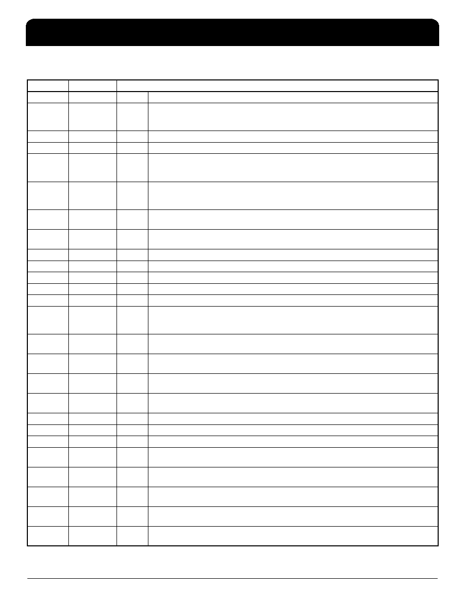
Table 1. Pin Descriptions
NOTE: Pullup refers to internal input resistors. See Table 2, Pin Characteristics, for typical values.
Number
Name
Type
Description
1
GNDI
Power
Power supply ground.
2
nMR/OE
Input
Pullup
Master reset and output enable. When HIGH, enables the outputs.
When LOW, resets the outputs in a high-impedance state and resets output divide
circuitry. Enables and disables all outputs. LVCMOS / LVTTL interface levels.
3
FRZ_CLK
Input
Pullup
Clock input for freeze circuitry. LVCMOS / LVTTL interface levels.
4
FRZ_DATA
Input
Pullup
Configuration data input for freeze circuitry. LVCMOS / LVTTL interface levels.
5,
26,
27
FSEL_FB2,
FSEL_FB1,
FSEL_FB0
Input
Pullup
Select pins control Feedback Divide value. LVCMOS / LVTTL interface levels.
See Table 3B.
6
PLL_SEL
Input
Pullup
Selects between the PLL and reference clocks as the input to the output dividers.
When HIGH, selects PLL. When LOW, bypasses the PLL and reference clocks.
LVCMOS / LVTTL interface levels.
7
REF_SEL
Input
Pullup
Selects between CLK0 or CLK1 and CLK, nCLK inputs. When LOW, selects CLK0
or CLK1. When HIGH, CLK, nCLK inputs. LVCMOS / LVTTL interface levels.
8
CLK_SEL
Input
Pullup
Clock select input. When LOW, selects CLK0. When HIGH, selects CLK1.
LVCMOS / LVTTL interface levels.
9, 10
CLK0, CLK1
Input
Pullup
Single-ended reference clock inputs. LVCMOS/LVTTL interface levels.
11
CLK
Input
Pullup
Non-inverting differential clock input.
12
nCLK
Input
Inverting differential clock input. VDD/2 default when left floating.
13
VDDA
Power
Analog supply pin.
14
INV_CLK
Input
Pullup
Inverted clock select for QC2 and QC3 outputs. LVCMOS / LVTTL interface levels.
15, 24, 30,
35, 39, 47,
51
GNDO
Power
Power supply ground.
16, 18,
21, 23
QC3, QC2,
QC1, QC0
Output
Single-ended Bank C clock outputs. LVCMOS/ LVTTL interface levels.
17, 22, 33,
37, 45, 49
VDDO
Power
Output power supply pins.
19,
20
FSEL_C1,
FSEL_C0
Input
Pullup
Select pins for Bank C outputs. LVCMOS / LVTTL interface levels. See Table 3A.
25
QYSNC
Output
Synchronization output for Bank A and Bank C. Refer to Figure 1, Timing Diagrams.
LVCMOS / LVTTL interface levels.
28
VDD
Power
Power supply pin.
29
QFB
Output
Single-ended feedback clock output. LVCMOS / LVTTL interface levels.
31
EXT_FB
Input
Pullup
External feedback. LVCMOS / LVTTL interface levels.
32, 34,
36, 38
QB3, QB2,
QB1, QB0
Output
Single-ended Bank B clock outputs. LVCMOS/ LVTTL interface levels.
40,
41
FSEL_B1,
FSEL_B0
Input
Pullup
Select pins for Bank B outputs. LVCMOS / LVTTL interface levels. See Table 3A.
42,
43
FSEL_A1,
FSEL_A0
Input
Pullup
Select pins for Bank A outputs. LVCMOS / LVTTL interface levels. See Table 3A.
44, 46
48, 50
QA3, QA2,
QA1, QA0
Output
Single-ended Bank A clock outputs. LVCMOS/ LVTTL interface levels.
52
VCO_SEL
Input
Pullup
Selects VCO. When HIGH, selects VCO ÷ 1. When LOW, selects VCO ÷ 2.
LVCMOS / LVTTL interface levels.
发布紧急采购,3分钟左右您将得到回复。
相关PDF资料
ICS87973DYILFT
IC CLK MULT/ZD BUFFER 52-LQFP
ICS87974CYILF
IC CLK GEN LVCMOS/LVTTL 52-LQFP
ICS894D115AGI-04LF
IC CLK/DATA RECOVERY 20-TSSOP
ICS894D115BGI-01LF
IC CLK/DATA RECOVERY 20-TSSOP
ICS9112AM-17LF
IC BUFFER HI PERFORMANCE 16-SOIC
ICS91305AMILF
IC CLOCK DRIVER LO JITTER 8-SOIC
ICS91305AMLF
IC CLOCK DRIVER LO JITTER 8-SOIC
ICS91309AGILF
IC CLK BUFFER ZD PLL 16TSSOP
相关代理商/技术参数
ICS87973DYI-147LFT
功能描述:IC CLK MULT/ZD BUFFER 52TQFP RoHS:是 类别:集成电路 (IC) >> 时钟/计时 - 时钟发生器,PLL,频率合成器 系列:HiPerClockS™ 标准包装:1,000 系列:- 类型:时钟/频率合成器,扇出分配 PLL:- 输入:- 输出:- 电路数:- 比率 - 输入:输出:- 差分 - 输入:输出:- 频率 - 最大:- 除法器/乘法器:- 电源电压:- 工作温度:- 安装类型:表面贴装 封装/外壳:56-VFQFN 裸露焊盘 供应商设备封装:56-VFQFP-EP(8x8) 包装:带卷 (TR) 其它名称:844S012AKI-01LFT
ICS87973DYILF
功能描述:IC CLK MULT/ZD BUFFER 52-LQFP RoHS:是 类别:集成电路 (IC) >> 时钟/计时 - 时钟发生器,PLL,频率合成器 系列:HiPerClockS™ 标准包装:2,000 系列:- 类型:PLL 频率合成器 PLL:是 输入:晶体 输出:时钟 电路数:1 比率 - 输入:输出:1:1 差分 - 输入:输出:无/无 频率 - 最大:1GHz 除法器/乘法器:是/无 电源电压:4.5 V ~ 5.5 V 工作温度:-20°C ~ 85°C 安装类型:表面贴装 封装/外壳:16-LSSOP(0.175",4.40mm 宽) 供应商设备封装:16-SSOP 包装:带卷 (TR) 其它名称:NJW1504V-TE1-NDNJW1504V-TE1TR
ICS87973DYILFT
功能描述:IC CLK MULT/ZD BUFFER 52-LQFP RoHS:是 类别:集成电路 (IC) >> 时钟/计时 - 时钟发生器,PLL,频率合成器 系列:HiPerClockS™ 标准包装:1,000 系列:- 类型:时钟/频率合成器,扇出分配 PLL:- 输入:- 输出:- 电路数:- 比率 - 输入:输出:- 差分 - 输入:输出:- 频率 - 最大:- 除法器/乘法器:- 电源电压:- 工作温度:- 安装类型:表面贴装 封装/外壳:56-VFQFN 裸露焊盘 供应商设备封装:56-VFQFP-EP(8x8) 包装:带卷 (TR) 其它名称:844S012AKI-01LFT
ICS87974CYILF
功能描述:IC CLK GEN LVCMOS/LVTTL 52-LQFP RoHS:是 类别:集成电路 (IC) >> 时钟/计时 - 时钟发生器,PLL,频率合成器 系列:HiPerClockS™ 标准包装:1,000 系列:- 类型:时钟/频率合成器,扇出分配 PLL:- 输入:- 输出:- 电路数:- 比率 - 输入:输出:- 差分 - 输入:输出:- 频率 - 最大:- 除法器/乘法器:- 电源电压:- 工作温度:- 安装类型:表面贴装 封装/外壳:56-VFQFN 裸露焊盘 供应商设备封装:56-VFQFP-EP(8x8) 包装:带卷 (TR) 其它名称:844S012AKI-01LFT
ICS87974CYILFT
功能描述:IC CLOCK GEN 1-15 PLL 52-LQFP RoHS:是 类别:集成电路 (IC) >> 时钟/计时 - 时钟发生器,PLL,频率合成器 系列:HiPerClockS™ 标准包装:1,000 系列:- 类型:时钟/频率合成器,扇出分配 PLL:- 输入:- 输出:- 电路数:- 比率 - 输入:输出:- 差分 - 输入:输出:- 频率 - 最大:- 除法器/乘法器:- 电源电压:- 工作温度:- 安装类型:表面贴装 封装/外壳:56-VFQFN 裸露焊盘 供应商设备封装:56-VFQFP-EP(8x8) 包装:带卷 (TR) 其它名称:844S012AKI-01LFT
ICS879893AYILF
功能描述:IC CLK GEN LVCMOS/LVTTL 48-LQFP RoHS:是 类别:集成电路 (IC) >> 时钟/计时 - 时钟发生器,PLL,频率合成器 系列:HiPerClockS™ 标准包装:1,000 系列:- 类型:时钟/频率合成器,扇出分配 PLL:- 输入:- 输出:- 电路数:- 比率 - 输入:输出:- 差分 - 输入:输出:- 频率 - 最大:- 除法器/乘法器:- 电源电压:- 工作温度:- 安装类型:表面贴装 封装/外壳:56-VFQFN 裸露焊盘 供应商设备封装:56-VFQFP-EP(8x8) 包装:带卷 (TR) 其它名称:844S012AKI-01LFT
ICS879893AYILFT
功能描述:IC CLK GEN LVCMOS/LVTTL 48-LQFP RoHS:是 类别:集成电路 (IC) >> 时钟/计时 - 时钟发生器,PLL,频率合成器 系列:HiPerClockS™ 标准包装:1,000 系列:- 类型:时钟/频率合成器,扇出分配 PLL:- 输入:- 输出:- 电路数:- 比率 - 输入:输出:- 差分 - 输入:输出:- 频率 - 最大:- 除法器/乘法器:- 电源电压:- 工作温度:- 安装类型:表面贴装 封装/外壳:56-VFQFN 裸露焊盘 供应商设备封装:56-VFQFP-EP(8x8) 包装:带卷 (TR) 其它名称:844S012AKI-01LFT
ICS87993AYILF
功能描述:IC PLL CLK DRIVER 1-5 32-LQFP RoHS:是 类别:集成电路 (IC) >> 时钟/计时 - 时钟发生器,PLL,频率合成器 系列:HiPerClockS™ 标准包装:1,000 系列:- 类型:时钟/频率合成器,扇出分配 PLL:- 输入:- 输出:- 电路数:- 比率 - 输入:输出:- 差分 - 输入:输出:- 频率 - 最大:- 除法器/乘法器:- 电源电压:- 工作温度:- 安装类型:表面贴装 封装/外壳:56-VFQFN 裸露焊盘 供应商设备封装:56-VFQFP-EP(8x8) 包装:带卷 (TR) 其它名称:844S012AKI-01LFT